
“Aging” refers to the natural process wherein X7R, X5R, Z5U & Y5V ceramic capacitors exhibit a drop in capacitance and dissipation factor over time. It is caused by a gradual realignment of the crystalline structure of the ceramic. To reverse this shelf life aging effect, the parts can be “deaged” by baking parts at +125ºC for 4 hours or ½ to 1hour at +150ºC. This will result in parts increasing in capacitance and returning closely to their original value. It should be noted that parts which are deaged and then subjected to temperatures above the curie point (typically +120ºC), such as soldering and temperature cycling, may shift up in value slightly. As the temperature is later reduced below the Curie point, the capacitance gradually returns to its previous values. Aging occurs at a rate that decreases roughly linearly with the log of time. NPO/C0G and tantalum capacitors have a different molecular structure which is essentially immune to aging and therefore they remain quite constant with time.
The aging rates are somewhat proportional to the dielectric constant or permittivity of a materials and are typically expressed as a percent per decade hour (i.e. 1-10 hours, 10-100 hours, 100 – 1000 hours, etc. Aging occurs quickly at first and then much more slowly over time. Maximum aging rates are as follows:
Maximum % Capacitance Loss/Decade Hour
X7R – 2.0%
X5R – 2.5%
Z5U – 7.0%
Y5V – 7.0%
(actual rates may be lower)
Because the capacitance changes rapidly just after deaging, capacitance measurements are delayed for 24 hours (referred to as “last heat”).
Parallel: When connected in parallel, the total capacitance is equal to the sum of the individual capacitance values. When connected in series, the total capacitance is lowered to the reciprocal level (exactly the opposite of resistors). For example, if three capacitors of values 1.0µF, 0.10µF, and 0.010µF are connected in parallel, the total capacitance would be:
C = C1 + C2 + C3 = 1.0µF + 0.10µF + 0.010µF = 1.11µF
The voltage rating of the parallel capacitors is only as high as the smallest voltage rating of the group, if they aren’t equal. If they are equal, the voltage rating is the same as that of a single capacitor.
Series: If the same three capacitors are connected in series, add their reciprocal values, as follows:
1/C = 1/C1 + 1/C2 + 1/C3 = 1/1 µF + 1/0.1µF + 1/0.01µF = 1/0.009, therefore C = 0.0090µF
The voltage rating of the series capacitors is equal to the sum of the voltage ratings of the individual capacitors if they are the same value. If the capacitors are of different values, and are used in an AC circuit, the voltage division will not be equal.
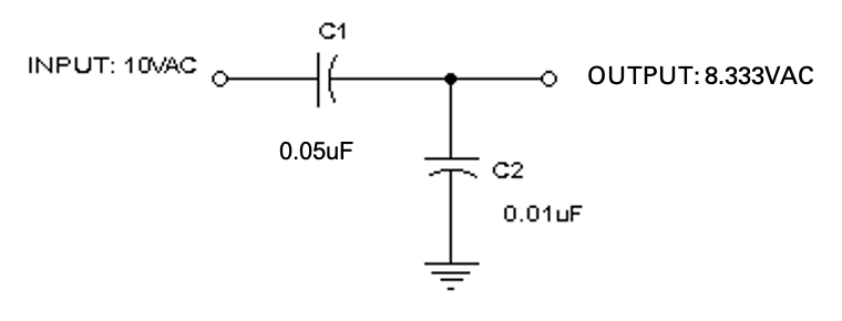
AC Voltage Divider: Capacitive dividers can be used with AC input signals. Since a DC input voltage wouldn’t pass through the capacitors, the DC case isn’t relevant. The formula for determining the AC output voltage of a capacitive divider is as follows:
Vout = (Vin * C1) / (C1 + C2)
Example: In the following circuit, the output voltage would be: Vout = (10VAC x 0.050µF)/(0.050µF + 0.010µF) = 8.333VAC. The output voltage is typically not dependent on the input frequency however, if the reactance of the capacitors is too low at the frequency of interest, the output current capability will also be very low.
On a Tantalum capacitor with radial leads (RCD TR Series), the long leg lead is always the positive or anode lead on the capacitor. The capacitor should also have the polarity marked on the capacitor. The exception to this is a non-polar capacitor (such as RCD’s CEA or CER Series ceramic capacitors) which will have no polarity marking on them. Non-polar capacitors may still have different lead lengths but this does not indicate any polarity orientation.
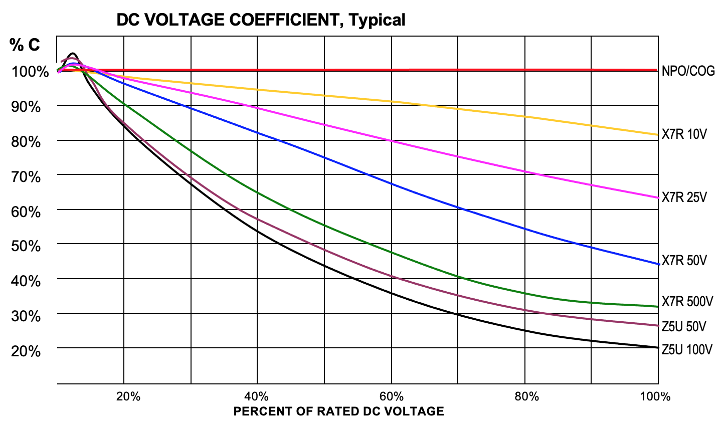
Class 2 (X7R, X5R) and Class 3 (Y5V,Z5U) ceramic capacitors have problems not seen in Class 1 (NPO, COG) and film capacitors, including very poor temperature drift, high voltage-coefficient-of-capacitance and, high voltage-coefficient-of-dissipation factor (all of these are different for AC and DC), high frequency-coefficient-of-capacitance and a significant aging rate.
Class 2 capacitors are best suited for coupling (DC blocking) and power supply bypassing. They are primarily used in linear applications where performance and stability are of no great concern. Class 3 capacitors should be used only for DC blocking and bypassing. The change in capacitance due to aging, temperature coefficient, and voltage coefficient must be taken into account whenever using Class 2 or 3 caps, especially class 3. For best performance, use the parts at a low percentage of rated voltage.
Applied voltage affects some properties so much that these capacitors are normally characterized at no more than 1 volt AC or DC. The table below shows what happens to capacitance when DC voltage is applied to various ceramics. Capacitance vs. AC voltage generally has the opposite result (capacitance increases in value). The numbers are approximate and vary somewhat with capacitance value.
Ceramic capacitors are quite reliable. Failures typically result from voltage overloads or mechanical stress. The most commonly reported cause of field failures is high leakage (i.e., low insulation resistance) usually attributable to microcracks. When high energy levels are involved, microcracks can result in catastrophic failure. Under lower energy levels, damaged chips could continue to function for a long time. Circuit test equipment will generally only identify those caps with high leakage levels. The reason for this is because the crack (or more specifically the air gap in the dielectric resulting from the crack), acts as a capacitor, making the damage difficult to detect. Since the voltage stress is concentrated in the area of the crack, this degrades the bulk resistivity, propagating even higher leakage levels over time especially in conditions of high temperatures and humidity.
Causes of cracks are typically due to mechanical stresses (excessive board flex, shock/vibration impact from handling, testing, depanelization, pick & place pressure, etc.), or thermal stresses (excessive soldering temperature or duration, thermal expansion/mismatch). In addition to user-related problems
Failures can also result from:
- improper surface conduction, i.e., entrapped flux under chip or external surface contamination (more common with “No clean” systems) result in shunt leakage paths.
- Fractured terminations
- High surge currents
- Aging – the capacitance value typically decreases through the normal aging process on X5R, X7R, Z5U, Y5V dielectrics.
- Voltage and temperature changes can also have a fairly significant affect on the capacitance value of these dielectrics resulting in parts which have temporarily shifted beyond the nominal tolerance band
- Open/intermittent solder joints due to tombstoning, poor PCB or chip solderability, leaching of the termination plating, chip or solder placement, cold solder joints, etc.
- Improper handling or processing by the capacitor manufacturer can result in cracks or voids in dielectric.
- Improper labeling or sorting by manufacturer
Note: it is not uncommon for the nodal analysis by ICT (In-Circuit Test) equipment to falsely characterize a chip capacitor as being non-compliant when another component is actually at fault.
The 3-character designations describe how a particular type of ceramic capacitor will perform over its intended temperature range. See breakdown in following table. The code was assigned by the Electronic Industries Association (EIA).
Lowest Operating Temperature | Highest Operating Temperature | Maximum Allowable Capacitance Shift from 25ºC Readings | |
Without DC Bias | At 50% rated V | ||
X = -55ºC | 5 = 85ºC | R = +15/-15% | R = +15/-15% |
Z = +10ºC | 7 = 125ºC | S = +22/-22% | S = +22/-22% |
Y = -30ºC | 8 = 150ºC | U = +22-56% | U = +22-56% |
V = +22/-82% | V = +22/-82% | ||
Precision capacitors are identified as COG (also known as NPO) which indicates a worst case temperature coefficient of 30PPM/ºC (0.003%/ºC).
- Advise competitor’s part number or, if unavailable, advise whether it is a conventional thru-hole part (axial, radial or disc) or surface mount.
- Advise construction (ceramic, tantalum, etc.). If unknown, go to #3.
- Advise capacitance value (0.01µF or micro farads, 10nF or nano farads, etc.).
- Advise capacitance tolerance (“Z “or +80/-20%, 10%, 5%, etc.).
- Advise voltage rating (50V, 6V, etc.).
- Advise dielectric (if a ceramic). NP0/C0G, X7R, Y5V, Z5U, X5R, etc.
- Advise of any special electrical requirements (low ESR, low profile, marking, etc.).
- Advise of any special lead-forming if thru-hole.
- Advise of any special packaging requirements (bulk, tape/reel, etc.).
Carbon comp resistors can shift in value from overheating so yes, they might be overheating during your soldering process. They also increase in resistance due to moisture absorption. Refer to Table 1 for the recommended preconditioning schedule to bake out the moisture. Lastly, carbon comp resistors can also shift up quite a bit if excessive strain is applied to lead wires (such as using a bending tool or machine that doesn’t provide strain relief, bending too close to body, etc.).
Carbon comp resistors are great for withstanding power overloads but unfortunately are more sensitive than most other resistors in regard to environmental or physical factors such as temperature, humidity, lead stress, etc. Try to minimize soldering heat and moisture absorption but most importantly, be careful not to impart any stress inside the body when forming the leads or mounting to PCB.
If the carbon comp resistor doesn’t meet the stability requirements of the circuit, contact RCD engineering to determine whether there’s another resistor construction available that will meet all the requirements. If surge is involved this might require a larger body size.
As carbon composition resistors absorb moisture their resistance increases over time, as the resistor approaches saturation. Under high humidity conditions it is not unusual for parts to increase 6% in resistance in as little as 72 hours.
As the carbon compositions are dried their resistance decreases over time. Reversing the effect of moisture on the part’s resistance is accomplished by storing them in a controlled low humidity area or by conditioning them in a convection oven at 100°C.
| Rating | Conditioning time @ 100°C |
|---|---|
| 1/8W | 25 hours |
| 1/4W | 50 hours |
| 1/2W | 75 hours |
| 1W | 120 hours |
| 2W | 130 hours |
 |  |
| Concave Terminations (RCD CN Series) | Convex Terminations (RCD SMN Series) |
Chip arrays are available in two styles (as illustrated above). The concave chip arrays (RCD CN series) have recessed terminations whereas the convex arrays (SMN series) have protruding terminations. Some resistor manufacturers offer only one type and some offer the other (more offer convex than concave).
Some customers prefer one type, some the other (convex is more popular). RCD originally offered only the convex version (1985) but later developed the concave version (1991) in order to meet the requirements of all customers. The convex version is generally the lower-cost version resulting from greater popularity and higher production volumes.
Some customers prefer the convex version due to larger clearance between terminations (typically 0.3mm vs. 0.25mm) which reduces the likelihood of solder bridging and short circuits. Another advantage of the convex termination is that optical inspection is faster and easier since the terminations are clearly visible instead of being embedded within the outline of the chip.
Some customers have found that the concave geometry offers superior self-alignment of skewed components during reflow soldering, yet others have found that the larger termination area of convex parts enhances self-alignment. RCD doesn’t take a position in which is “better” but can offer samples of both for customer evaluation.
Operation at high altitudes can cause increased self-heating as well as corona and arcing, especially if moisture is present. All of RCD’s standard catalog resistor models will operate at altitudes of 50,000 feet (equates to a pressure of 3.44 inches of mercury). Some models are available to 100,000 feet or higher (0.315 inches of mercury). When standard resistors aren’t suitable, RCD can generally offer custom-designed options for operation at even greater altitudes. RCD’s Test Lab can perform specific test screening for customers using precision vacuum equipment.
Since performance is affected by altitude, the general rule of thumb recommended by RCD to ensure safe and reliable operation is to derate the power/voltage/current ratings by 10% to 20% per 10,000 feet.
As for depths below sea level, RCD has not evaluated products but has been advised that various resistors function well at -500 ft (30.47 inches of Hg).
Resistors specifically designed for high surges are best, such as composition styles are best (refer to RCD series CC, PR, PRM, PCN). Without going to a specialty resistor the customer should concentrate on wirewound resistors, followed by thick film resistors. Thin film resistors tend to be the most sensitive although they are generally OK in most applications. Larger sizes enable greater ESD capability. RCD specializes in pulse-tolerant resistors and can assist in product selection.
No, only those resistors with a suitably high resistance value (at or above the “critical resistance value”) may be operated at the maximum voltage rating.
Most resistors carry a RCWV (rated continuous working voltage) rating, also known as the Maximum Voltage Rating. This is the maximum DC or ACRMS (or ACPEAK on some resistor types) voltage that the resistor size is designed to withstand across its terminals, or across its internal construction. The actual working voltage for a particular part and resistance value is determined by the formula E=(PR) 1/2 , E (voltage) not to exceed the maximum RCWV.
For a given voltage and a given power rating there is only one value of resistance that will dissipate full rated power at rated voltage. This value of resistance is commonly referred to as the “critical resistance”. For values of resistance below the critical value, the maximum (element) voltage is never reached and, for values above the critical value, the power dissipated becomes lower than rated. As such, the resistor power and voltage ratings are an “either/or” rating, i.e. resistors are limited by their power rating (typically lower resistance values) or by their voltage rating ( higher values), whichever is less.
Example: RCD type MC1206 20,000 ohm chip resistor has a power rating of 0.25W and a Max Voltage Rating of 200V. Can the part be operated at 200V? The answer is “no” because 200V across 20,000 ohms equates to 2 watts (P=E2/R so P=2002/20,000= 2 watts). At 200V the parts would quickly overheat since this is 8 times the wattage rating! The actual working voltage of MC1206 100 ohm is determined by E=(PR) 1/2 or (.25 x 20,000)1/2 = 70.7V.
RCD offers a wide range of customized voltage options via use of specialty materials and designs if the standard voltage rating isn’t adequate. These specialty designs can typically offer 50% to 200% increases in voltage levels above standard models.
Unless specifically prearranged before ordering, there is no guaranteed resistance tracking/matching level. Parts with an absolute tolerance of 1% therefore will track within a range of 2% (i.e. – 1% to +1%). Nothing better is guaranteed or implied. In actuality though, if all parts are manufactured at same time under the same conditions, the distribution will typically follow a somewhat normal bell curve, i.e., fairly normal Gaussian kurtosis approximately centered on the nominal resistance value. Some lots are skewed more toward high side of tolerance, others to low side. Other lots are more leptokurtic (tightly distributed) than others. On some occasions, 1% parts are binned from 5% orders, so these orders could have fairly flat or platykurtic curves. In order to guarantee a tightened matching level, simply advise your resistance matching requirements, so that RCD can quote and produce accordingly. Depending on the product, RCD can often achieve tolerance matching to 0.01% or tighter.
Unless indicated otherwise on data sheet, or specifically prearranged before ordering, there is no guaranteed TCR tracking level. Parts with an absolute TC of 10ppm therefore will track within a range of 20ppm (i.e. – 10 to +10ppm). In actuality though, if all parts are manufactured at same time under the same conditions, the TC might track much more closely. In order to guarantee a tightened tracking level, simply advise your TC tracking requirements, so that RCD quotes and produces accordingly. Depending on the product, RCD can often achieve TC tracking to 1ppm or tighter.
The level of outgassing depends on the product and loading conditions. When outgassing is a concern, we can utilize a special ceramic coating (on most products) which is supplied to a variety of aircraft and Space applications. We don’t have ability to test outgassing at our lab here but have been told by customers that it is excellent (less than 1% total mass loss and less than 0.1% volatile condensable material). We can supply samples for customer verification or send to an external Materials Test Laboratory (cost to be borne by customer).
The voltage coefficient is the temporary shift in resistance due to application of voltage across a resistor; typically measured at 10% rated V & 100% rated V, after correcting for self-heating effects. This is generally caused by molecular irregularities in the resistance element. It is similar to the temperature coefficient except voltage-based instead of temperature. It doesn’t relate to pulse capability (some parts with near-zero VC will shift far more and open sooner than other parts with relatively high VC’s).
One of the main purposes for knowing the VC is to improve circuit accuracy (especially in high voltage circuits). For instance, if a part has 10ppm VC (.001%/volt) then the part will shift from its nominal value by up to 1% at 1KV. That may be fine for a 10% circuit but obviously could present a severe problem to a 0.1% circuit.
RCD offers a wide range of customized options via the use of specialty materials and processing to achieve improved VC stability, if the standard rating isn’t adequate.
There are three basic precision resistor technologies… wirewound, thin film, and foil. Although there are some variations, the vast majority of parts in all three technologies utilize Nickel Chromium as the resistive material. There are very few firms that produce all three technologies, so keep in mind that the info received from other manufacturers might be slanted toward their respective products.
The oldest of these technologies is wirewound. RCD’s President, Louis J. Arcidy, was instrumental in the development and advancement of this technology since the early 1950’s. RCD was founded 4 decades ago to produce ultra-precision WW resistors, and still maintains a dominant position in this market. Wirewound resistors have traditionally been regarded as the “Cadillac” of the industry, and to this day are greatly preferred in some applications such as high-end audio and medical instrumentation. WW resistors have the greatest mass of resistance material which, with proper processing, results in highest stability, lowest noise, lowest VC, and greatest overload capability. It is this reason that nearly all Resistance Standards, i.e., those used by NIST and other Test Laboratories to calibrate precision measuring equipment, are wirewound technology.
Foil resistors evolved just after wirewounds and attracted a loyal customer base particularly in higher frequency applications due to low inductance and smaller PCB real estate. Foil technology has traditionally offered performance levels approaching that of wirewounds at pricing which was typically 20% more economical. Recent advances in foil technology have resulted in temperature coefficients that are equal or better than those of wirewounds, and thermal EMF’s that are approximately equal. The best wirewound resistors are typically 0.5 to 1ppm/E TCR, whereas some foil resistors are now available as low as .25ppm/EC. Very few applications require tighter than 1ppm to 5ppm so these can typically be filled by WW or foil technology.
Thin film resistors have encroached upon both WW and foil technology, and are particularly cost effective in less precise applications, i.e. tolerances of 0.020% to 0.10% and temperature coefficients in the range of 5ppm or larger. The pricing advantage over WW and foil technology is especially significant in higher resistance values (i.e., 100Kohm and above). Performance levels have steadily improved and although not quite at the level of WW and foil yet, are still suitable for many precision applications, especially in environmentally controlled environments, and applications without pulses/surges.
Precision wirewound resistors therefore are generally the best all-around choice for precision DC and low frequency AC applications (due to inherent inductance of WW construction, they are generally not suitable for high frequency applications). The major disadvantage of wirewound resistors (other than higher inductance level) has always been “pricing”, but with offshore production capability and advancements in automation, RCD’s wirewounds often now sell at a 20% discount to foil resistors instead of the traditional 25% premium! As a result, many customers have been switching away from film and even more so from foil technologies in favor of wirewounds over the past few years.
Yes, RCD’s silicone coated wirewound resistors (such as Series 100, 200, T, and RW) are compatible with aqueous cleaning systems however the coating is designed to be softer than others to enable the resistance wire to expand and contract in use (thereby offering greater stability and higher surge capabilities). Customers should avoid any harsh brushing or high pressure on parts. The parts should also be promptly dried after washing.
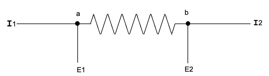
When current terminals I1 and I2 are connected to load, the voltage flows through terminal I1, then through the current sensing resistor element, and the other current terminal (I2). The same voltage is generated between terminal E1 and terminal E2 as well as at the both ends of the current sensing resistor. This voltage enables the detection of the flowing current.
Current [I] = Voltage [E] / current sensing resistance [R]
Though voltage generates at the terminals in a current circuit, it is not included in a voltage sensing circuit so it need not be considered. The terminal resistance (aE1 and bE2) is quite small related to impedance in a voltage sensing circuit, so it is possible to measure the current accurately without any consideration about resistance.
Refer to Engineering Report R-31 for additional information.
Our general rule of thumb for is to have approximately a 13mm (1/2″) clearance between the body of resistor and any combustible materials. Some customers utilize much smaller clearances depending on the PCB material and the fault condition. If the only possible fault is one in which the resistor will fuse very quickly, then there shouldn’t be enough time for the generated heat to transfer to PCB or nearby components. If however the fault could conceivably result in the resistor “hanging in” for seconds or minutes, then the resistor body could reach very high temps before fusing and could char or ignite the PCB or nearby components. If unable to achieve the recommended clearance, customers should evaluate prototypes under worst case conditions. Even a very small clearance such as 1mm would be far better than mounting the resistor body directly on the PCB since the air space acts as an insulator. Fuse resistor models which include a built-in thermal cutoff (such as RCD’s TF and LF Series) will not achieve the same temperature extremes and therefore can generally be mounted closer to the PCB and adjacent components.
Power wirewound resistors are often utilized in fairly high voltage applications (pulse or continuous). Since the breakdown voltage of most models is 1000’s of volts per centimeter of length, high voltage levels can be achieved with long body lengths, particularly in applications where substantial inductance isn’t a problem. If the resistor is subjected to an excessive amount of voltage or energy, the failure mode for these resistors can cause catastrophic damage to other components.
A wirewound resistor is made by winding a fine resistance wire, such as Nichrome, on a ceramic rod. If a small open develops in the winding due to excessive power/voltage/energy level, an arc will form at the gap, melting the wire back, making the arc bigger. As the process continues, the results can be rather explosive especially at high voltage levels. And since the failure mode can be a partial or full short through the resistor, it is likely that additional components in the circuit will be damaged. Never exceed the resistor’s ratings. RCD generally offers both continuous and short-term ratings (since resistors are capable of overloads for short periods). Our engineers are always available to assist in product selection. In some instances, a slightly modified design can result in a large increase in overload capability for little or no extra cost.
Composition resistors are great for applications that require special performance characteristics such as high surge energy, high peak pulse voltage, low inductance, high operating frequency, and non-magnetic construction. However in normal-use applications, they tend to be less stable than other resistor types, especially in the presence of moisture/thermal/voltage gradients. Composition resistors are the only Mil-spec product for which an “out-of-tolerance” condition is actually expected and specifically addressed in the Military drawing (MIL-R-39008)…
“6.9 Out-of-tolerance resistors. Resistance shifts due to absorption of moisture are inherent”.
As a result of this instability, the drawing specifies that the out of tolerance resistors be pre-conditioned in a dry oven at a temperature of 100ºC ±l5ºC for 96 ± 14 hours in order to obtain a more accurate measurement. Since composition resistors can rapidly shift out of tolerance, and since users generally don’t want to bother with the preconditioning processes, it is common to specify a tolerance tighter than actually needed (i.e. 5% tolerance if 10% is actually required, or 10% tolerance if 20% is required).
Composition resistors also tend to be more costly than other models, so if not needed for any of the special performance characteristics, customers should consider other models (consult RCD Engineering for application assistance).
Depending on the product, increased ratings are typically achieved via special materials and/or processing, much of which has been developed over the past 30+ years as a specialty component manufacturer. The details are proprietary but a brief description of each follows. Please note that in addition to the increased ratings that may be listed as Options on the data sheets, RCD can often achieve even higher wattage, voltage, amperage, dielectric, and overload levels (this extra level of performance can sometimes add significantly to the unit price).
Power: Increased power ratings are achieved primarily via use of materials with improved thermal conductivities. For instance, to improve a conventional leaded-wirewound resistor, the core, caps, leads, and coating material may all be optimized to enable a greater transfer of heat out of the resistor body into the surrounding air or through the lead wires into the PCB. Surface mount chips, such as MC2512B (2W in 1W package) and MLB2512 (3W in 1W package) also utilize such techniques as heavier/wider terminations, greater resistance layer mass/surface area, and specialized trimming to prevent hot spots and current crowding. The suggested mounting footprint is typically larger than conventional product to aid the thermal transfer. Some products also receive special processing and high-temp preconditioning to ensure stability at the elevated power levels.
Voltage: Increased working voltages may be achieved by utilizing special high voltage insulations and by modifying the element geometry to prevent internal arcing.
Amperage: Increased current ratings often involve heavier-duty terminals and internal design. This is often achieved by utilizing heavier gauge resistance wire, high thermal conductivity materials, and/or terminals with reduced resistivity and greater mass.
Dielectric Strength: Increased DWV (dielectric withstanding voltage) is generally achieved by utilizing materials with greater voltage capability, or by increasing the insulation thickness using standard materials.
Overload: RCD’s products are generally capable of brief overloads. In order to increase the power, voltage, and/or duration of the overload, RCD will often utilize a combination of special materials and processing. This may involve larger internal elements, heavier gauge resistance wire or film thickness, different resistance alloys or film compositions with higher voltage or current-carrying capabilities, higher melting points, special preconditioning, customized winding/ trimming/calibration, etc.